Kicad settings for cheap PCBs
08 September 2023 at 3:06 pm
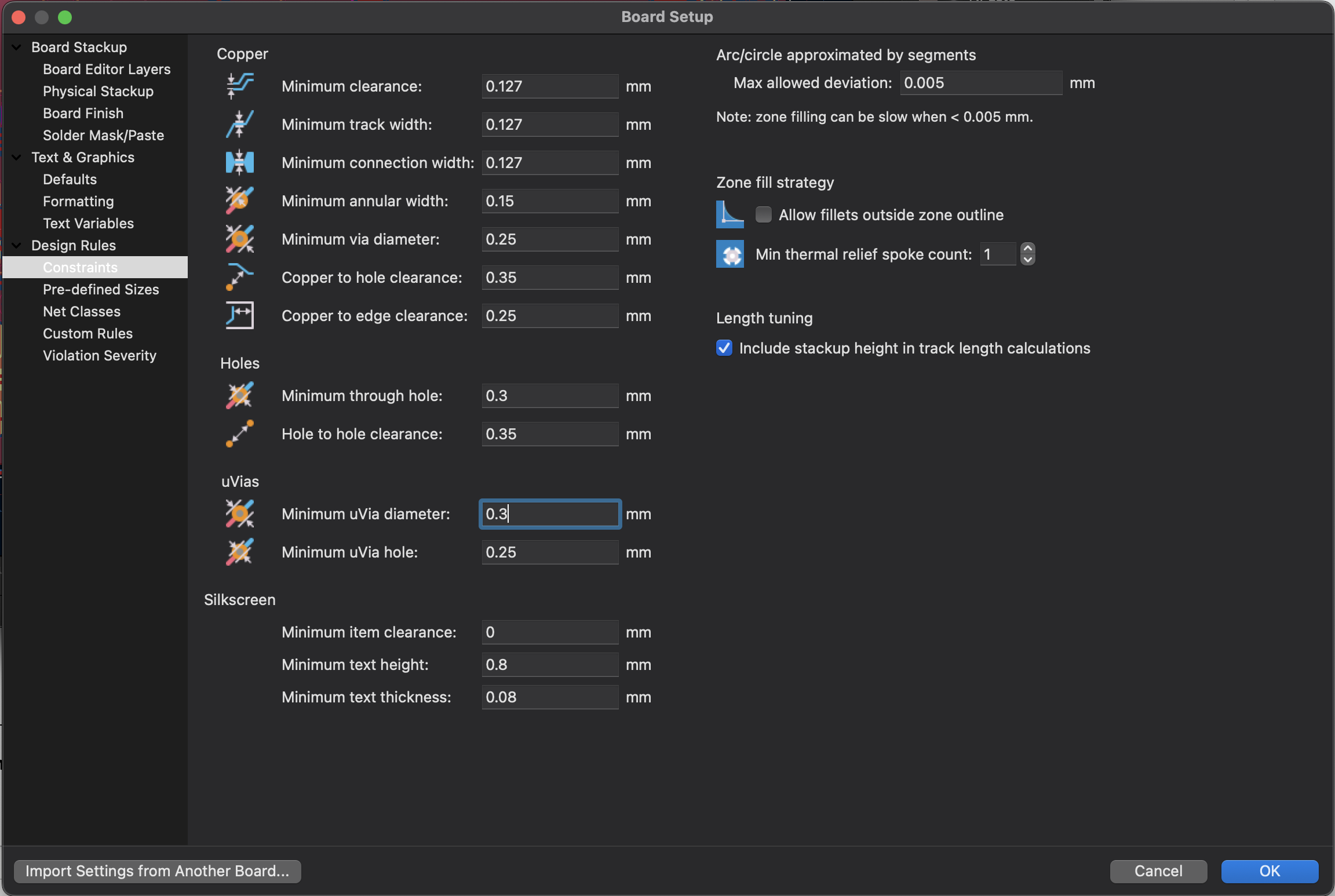
If you use the default Kicad settings, you’re probably fine with most PCB services, but I just ordered PCB’s that were 5 times the normal cost due to not knowing what can make your PCB not poolable (Standard PCB). This post lists the exact requirements & settings for your board to be poolable & still cheap when using Kicad and get your boards from PCBWay. I made this as a table so if you have the exact data for other vendors, message me and I’ll add it?
It’s all about the capabilities. PCBWay is listing their capabilities, but they don’t tell you exactly what will increase the price of the PCBs. If you use these settings in your Board Setup, your board is guaranteed to get the lowest possible price and close to $1 per board (at low volumes). If you buy thousands of boards it’ll drop down to $0.1 per board, but if you select the wrong options, you’ll easily pay $10 per board.
So in all cases, you’ll likely want to keep within these limits to retain that low price:
| Setting |
Value |
|---|---|
| Minimum clearance (track to track) |
0.127 mm (5 mil) |
| Minimum track width |
0.127 mm (5 mil) |
| Minimum connection width |
0.127 mm (5 mil) |
| Minimum annular width |
0.15 mm |
| Minimum via diameter |
0.25 mm |
| Minimum copper to hole clearance |
0.35 mm *) |
| Copper to edge clearance |
0.25 mm |
|
|
|
| Minimum through hole |
0.3 mm |
| Hole to hole clearance |
0.35 mm *) |
|
|
|
| Minimum uVia diameter |
0.3 mm |
| Minimum uVia hole |
0.25 mm |
*) If they are in the same net, it is 0.2mm. If not, it is 0.35. For PTH,it is 0.55mm, For standard pcb)
You must also select only the standard colors (green, red, yellow, blue, white and black) with their standard silkscreen color. This will increase production time, but not the price. As soon as you deviate from this, things will cost more. The reason is that this will cause special handling for this board. You would think that boards within the standard handling is what they call “Standard PCB”, but that’s not the case.
What I found the most confusing about the capabilities page is that the word “Standard PCB” may include many features that others might call “advanced” that will increase the price significantly. In my case, I used 0.2mm drill holes since these were listed as a “Standard” feature. This increased the price of each board from $1 to $10 per board, so I wanted to document what settings to use to still get cheap boards. Note that this primarily applies to low volume and prototyping. The more boards you order, the less this matters. For 5 boards, it causes an increase of 1000%. If I was ordering 5k boards it would only be a 15% extra for the same feature.
I’m really looking forward to receive the boards I just ordred! It’s a compact board for experimenting with I2S audio. I’ll use this for a customer project where I initially tried a different way to play audio (the VS1053 Codec). I2S is so much easier to integrate and for the price of a single VS1053 chip, I’m getting a ESP32-S3 based board with 16Mb Flash, line in, line out, headphone out and a 5W amplifier! These chips are so much more modern, so they need much less passives around them. If this dev board works well, I might even make it a product?
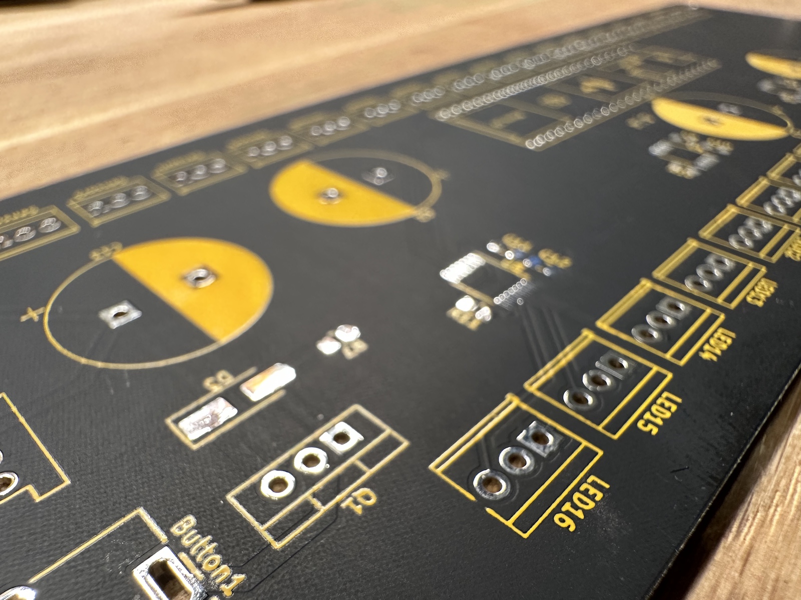
Also - I’m not always looking for the cheapest boards. Cheap boards are great for high volume or prototyping, but many features will drive cost. Some ICs only come in very small packages since they are made for the mobile phone business. Tiny chips with less than 0.2 mm between pins will drive the PCB cost though the roof! If space is at a premium, it’s usually worth it. Style also matters and can add cost. Here’s a board where my customer is a designer that cares about the appearance - black matte finish with yellow silkscreen. Love it!
Special features
I'll update this post as I discover more details about PCBWay's PCB capabilities (since they don't list it themselves):
For a specific board, I wanted a very thin PCB. As soon as you set the thickness to 0.2mm or 0.4mm, the price goes up significantly but so does the capabilities in terms of smallest possible board possible. If the thickness is greater than 0.5mm, the minimum PCB size is 5*5mm. If the thickness is less than 0.5mm, the minimum size can be 2*2mm, cut by laser.