Milling 2-sided PCB’s
08 January 2016 at 2:59 pm

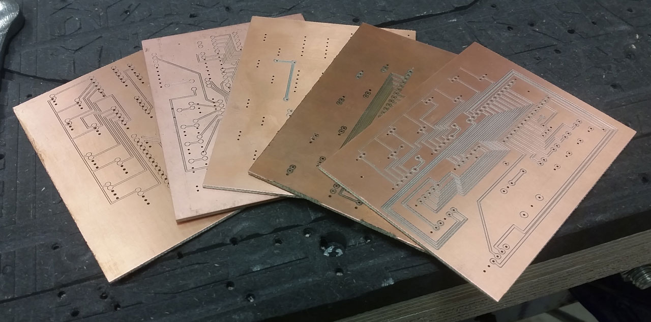
Before xmas I did a lot of PCB milling for a client. Compared to getting the PCB’s commercially made somewhere, this is the equivalent of rapid prototyping for circuits. Getting a board produced in the UK, Germany or Asia will typically take at least 2 weeks (but often 3). If you can reliably produce 2-sided boards using a mill, you’ll iterate and find errors faster.
Milling is a lot cleaner than etching and you really don’t want to hand-drill several hundred holes on an etched PCB. Getting perfect results every time took a bit of learning though, so I thought I’d describe my process for 2-sided boards here so others can use it.
Preparing the PCB
Unless I need components that only exist in Eagle, I make my boards using Fritzing since it’s quick and it has a great UI (compared to Eagle). Fritzing allows me to export both Gerber files for production and SVG files for home etching or milling. Fritzing is super easy to work with so I won’t go into details on it, but here’s some things to keep in mind when laying out the PCB.
When creating the layout, set the PCB to be the exact sub-millimeter size of your PCB milling blanks. Don’t be tempted to use a smaller size in the PCB design software since “you won’t need that much”. This will only give you headaches. Remember that using the size of the PCB blanks, you can easily add some cutting lines, so that when the PCB is perfect you can cut it to size. If you don’t do it like this, you can’t flip the board precisely enough. Trust me - I’ve tried and failed many times. It’s just not precise enough.
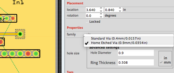
Many components in Fritzing such as via’s offer select a Home Etched version that is larger and easier to work with if you make the board yourself. You can also tweak components such as headers to be easier to mill.
One thing that isn’t obvious is that on a home-made board, it’s much easier to place components on the top and solder them all from the bottom of the board. Professionally made boards have through-hole plating so all holes are connected from top to bottom, but you won’t have this so all solder points should end up on the bottom in some way. You can still place traces on the top layer, but you’ll have to take them down to the bottom using a via for soldering. Don’t forget that rotating components makes a world of difference when laying out the PCB. If you manage to get the top layer as a solid ground plane with no vias, you’re saving a lot of manual labor.
A via for a homemade PCB is basically just a drill hole in which you solder a wire connected to both sides. Make sure to set the via to be large and not the tiny default used for professionally produced PCBs. This makes it much easier to solder them later.
Use the widest possible traces that will fit with the connectors and other components in your PCB design. The standard is to use 24mil traces. As we’ll be milling along the outline of the traces, so by using 32 or 48mil traces, you can run your mill on the outlines and still have a trace left. Alternatively, you can widen the traces in a vector editing program later, but I find it easier to do it straight in Fritzing.
The next important step is exporting the files (Export > For production > Etchable). This will export files for the silkscreen, paste mask, etch mask and copper traces. We only need the copper. What you’ll want is the “Copper top” and the “Copper bottom mirrored”. If you select the wrong files, you’ll have to redo (or mount the components on the “wrong” side of the board). I suggest that you print out these files on paper at 100% size, glue them together and cut to size so you get a “dummy” PCB before milling. Place your components onto it to see that it’s all correct from both top and bottom.
Preparing the output for milling
The exported SVG files will still need some “massaging” to work well. I use Adobe Illustrator, but you can also do this with free software as Inkscape. It just takes a little longer. First go into outline view so you can see any objects that the PCB software has placed two of. It’s quite common that square pads have a circular outline under them so clean this up.
Then merge all the vectors into solid shapes so that we can follow the outline to cut the trace out. Remember to copy the holes onto a separate layer before merging, so you have what you need for drilling the holes. I usually use the “Outline stroke” feature to turn lines into fills and then I’ll use the Pathfinder panel to Unite all the connected/overlapping vectors. Illustrator does this in seconds, but Inkscape can take 15 minutes for even simple boards.
When you have all the shapes merged into solids, you can move the file to your CAM software. At Bitraf, we use VCarve but all you need to do is to set up paths and drills based on the vector file you’ve made. I’m using a 90 degree V-bit for the traces and all I have to do is to follow the outlines and cut just deep enough to break connectivity. For the holes I use 0.8mm drills or 1mm if I’m to add through hole rivets like these http://www.ebay.co.uk/itm/200x-best-quality-pcb-copper-via-vias-through-hole-rivets-ID-0-8mm-OD-1mm-/321930742366?
Now that we have the files ready, it’s time to move on to the milling. For this project I used the huge Shopbot PRS Alpha that we have at Bitraf, but the process will be identical for any other mill.
How to make a good Jig
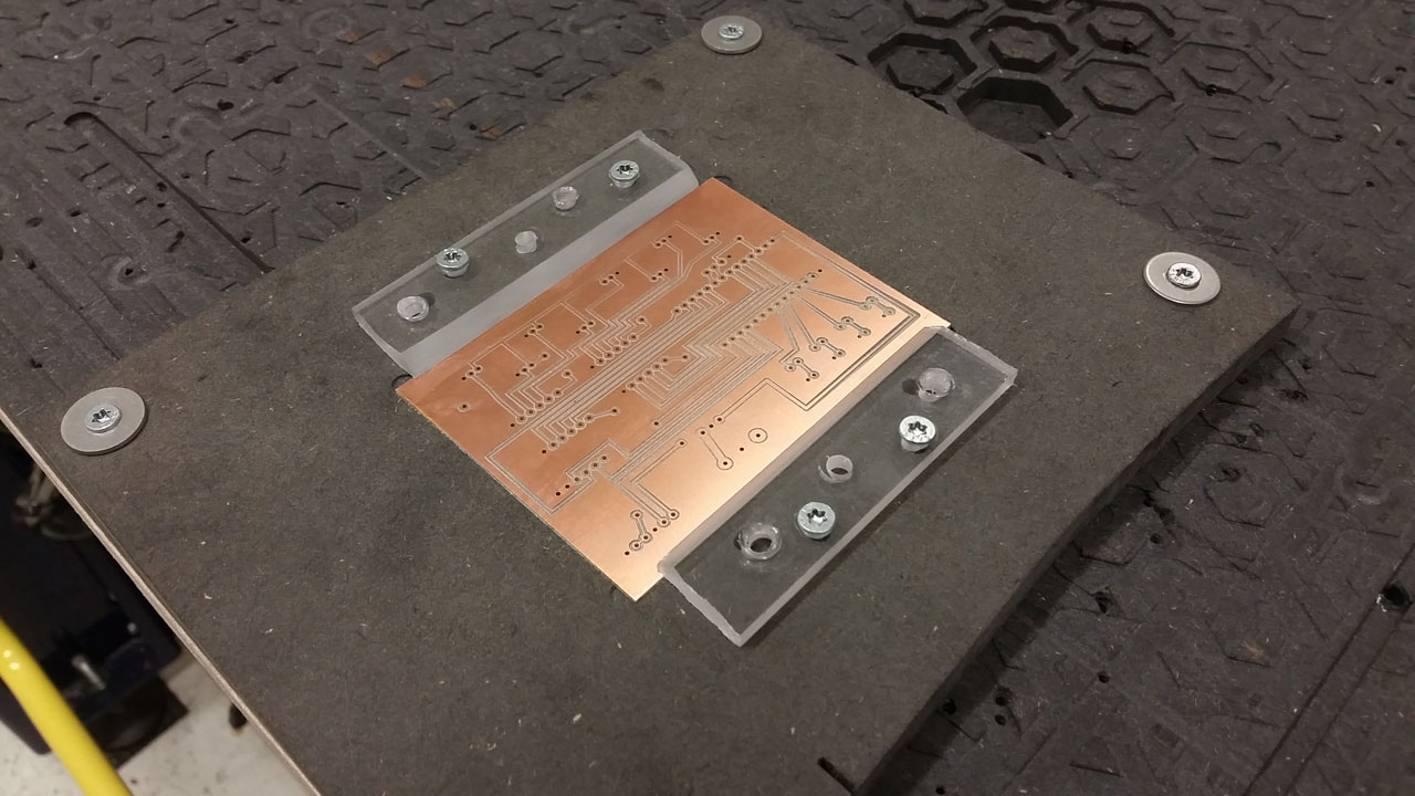
The entire secret to getting two sided PCBs perfect is to have a good “jig” - a setup that ensures 100% identical placement on both sides. I made my jig using a scrap piece of High Density Fiberboard (HDF) but you probably use can use many other materials for this.
- Fix a piece of fiber board blank to the drilling surface. This will become our jig. It should be somewhat bigger than the PCB itself.
- Use a mill to by mill away a millimeter or so of the surface. This will compensate for any deviations when mounting the fiber board blank and ensures the surface is 100% planar.
- If your PCB is 1.5mm thick, mill a pocket for the PCB that is a little less than the thickness of the PCB. I used 1.2mm, so the PCB was only sticking out a tiny bit. I made the entire pocket 0.05mm wider than the PCB and that gave me “push-fit”.
- If you’re making many copies of the PCB - mill a hole on the side of the pocket that is big enough for your finger, so you easily lift the boards out.
- Put the PCB in the pocket and make either a full frame (slightly smaller than the PCB) or use some small wooden pieces that you the fixate the board with. Don’t over-tighten as that can cause the PCB to become slightly bent giving you uneven
With this technique, your board will be 100% in the same place when you flip it around to do the other side. On the boards that I make now, I cannot see any sub-millimeter deviation from one side to the other.
I initially tried tape/glue rather than milling a pocket. The result was that I bent the boards ever so slightly and that caused some traces to get uneven widths since the mill went deeper. This approach of just holding the board down solves this.
The importance of having identical blanks
For the jig to work well it’s extremely important to have PCB blacks of identical size. Initially I was unable to find suitable size PCBs at my local electronics store, so I picked of some boards that were twice the required size and cut these in two. Despite using the mill, I didn’t get these to the exact size and it bit me later on. I waited until my supplier had restocked and then this was no longer an issue.
Signs that something’s wrong
Cutting 0.18 into the board should isolate the traces when using a 90 degree V-bit. If more is required, check alignment of the board in the jig! Twice I’ve spent hours on milling just to get the other side of the board wrong. Always start with the drills, then the layer with the least amount of traces (usually the top layer). This will give you the shortest route to seeing if things are correctly set up. Alternatively, do the drill holes from both sides to verify that they align.
I hope this helps others making two-sided milled boards. If you use the instructions, feel free to email me a picture of the jig & result?


