Kicad plugin that can shave hours off your PCB layout
29 August 2020 at 6:15 pm
Just before the summer holidays I was commissioned to do two fairly large PCB’s for a longtime customer. Both the boards had repeating elements and they both had about 300 components to lay out. When you start off your PCB layout in Kicad, it will import all the footprints as a huge “lump” and leave it to you to sort them. What if I could spend 3-4 hours on a script that could make this easier?
I’ve done this exercise before and completely missed my estimate, but this time it actually held up. TL:RD jump to the end to get the workflow that’ll save you hours, or read on to find out how I solved this.
I started by asking around if anyone knew a better way to do this, but I realised this had not yet been solved. I’m not very fluent in Python, but I can certainly bend it to do what I want and I thought that for simple text parsing like this it would be the right thing. Also - all Kicad plugins are written as Python, so maybe I could convert it to one?
My idea
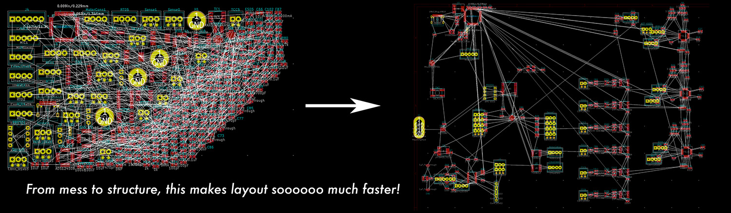
One of my favorite Kicad features is that all the files are plain text files. This makes them human readable and since they are well structured, you can also parse them easily. From having read the files, I knew that there is an unique component reference for each component and this is the same in both files. My very simple idea was thus to just copy the positions from one file to the other.
After a few hours of hacking, I got a script together that worked well and I shared it to get feedback and give back to the Kicad community. The feedback was very positive, so I also shared it on the Kicad forums.
The initial response there was that some of the regular members pretty much ignored the script, but rather commented that I should have used hierarchal layout. I was a little set back by this, but decided to ignore those comments since it seemed that these guys didn’t quite understand what I tried to solve. Others thought it was brilliant and even said it was so clever that they’d love to see it become part of Kicad, so I just focused on the positive comments.
Improving it
At this point it worked great for me, but Ian over at the Contextual Electronics forum wanted to take it further. Over the weekend, he turned it into a proper Kicad plugin and that makes it so much easier to use! To be honest - there’s not much left of my script - mostly just the idea, but this opens it up for so many more users to try it out and use it! We did some testing and it held up nicely and I could use it to lay out the first board. It was so much faster & very worth the time spent! I think I maybe save 2 hours on the first board alone?
I designed the other PCB using hierarchical sheets and when we tested that, we found a few edge cases that Ian solved swiftly.
How to use it
To shave hours of your layout time, just download and install the plugin using the SchematicPositionsToLayout.py script using the provided instructions @ Ian’s site. Then open an empty PCB and import from schematics. Execute the SchematicPositionsToLayout script and all the components lay out at the same positions as in the Schematic.This makes it so much easier to find and place components.
Now it’s time for the second timesaver - for any hierarchical layout you have (any repeating part), you can now place components for the first of these and replicate this layout using the Replicate Layout plugin. In my case, I had 7 stepper drivers that each had 16 supporting components. I laid out the first stepper and also did a little routing around the chip. Using the Replicate layout, I then replicated this to the other six stepper drivers. In just 30 minutes, I had already laid out 1/3rd of the board (100 components!). Amazing time savings and with the precisely repeated layouts - the boards also look better!