Teensy 3.6 design files in Kicad
17 March 2021 at 2:34 pm
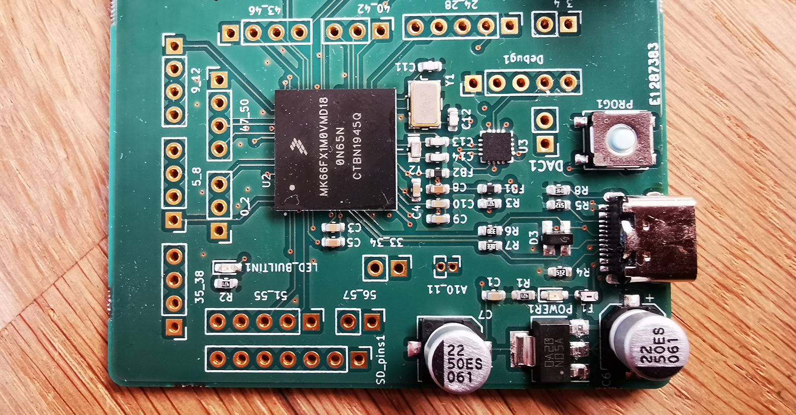
Back in July, I made a Teensy 3.2 reference design for those that want to make their own custom board. Now I’ve made a Teensy 3.5 / 3.6 design. This was my first board with a BGA chip, so I learned quite a lot in the process.
This breakout is based off a test board that I made for a customer. I made the customer board and then I removed all the customer specific parts so all 63 possible pins are broken out. You can find all the files in this GitHub repository. The picture above shows the final board I got from fab. This board differs from the original Teensy design in that I had no need for a SD card, so this makes pins 58-63 available for other things.
How to make 4 layer BGA’s cheap
When making 4 layer boards, it’s incredlibly important to stick with the manufacturers rules. Pooling of many boards in one big panel is what makes the price of PCB’s go down. If you design the board incorrectly, the board will fall out of this “pool” and be many times as expensive. In this case, I used Eurocircuits so the basic rule was - don’t use MicroVias and make the annular ring 0.3mm bigger than the size of the hole. Eurocircuits has this super-nice pre-flight tool for PCB’s, but despite changing all the vias to this, the preflight tests failed and the board became 10x expensive. In the end I found that you must use 0.5mm vias with 0.15mm drills to “fool” the “tool”, so vias must be 0.35mm bigger than the hole for the via.
Anyhow - I thought I’d publish the files for others to use as a starting point. Given that this was my first BGA layout, you might want to redo the routing, but it worked great for a first take! Also - I recommend checking out this YT video on laying out multi-layer boards. Lot’s of good tips!
Related: I’ve also updated my USB Type C repository with some alternate parts that match in terms of footprint.